The semiconductor industry's relentless pursuit of higher performance and reliability demands materials that can withstand extreme thermal and chemical environments while maintaining exceptional purity standards. Among these critical materials, high purity CVD Silicon Carbide (SiC) has emerged as a transformative solution for advanced semiconductor manufacturing processes, particularly in epitaxial growth, crystal production, and plasma etching applications.
Understanding High Purity CVD SiC Technology
Chemical Vapor Deposition (CVD) Silicon Carbide represents a sophisticated surface protection technology that applies ultra-pure SiC coatings to graphite components used in semiconductor manufacturing equipment. This advanced coating method addresses fundamental challenges in sub-micron semiconductor processes, including particle contamination control, thermal field stability, and chemical resistance in harsh reactor environments.
The CVD process deposits SiC molecules layer by layer onto graphite substrates, creating a dense, uniform protective barrier that exhibits extreme chemical inertness to aggressive gases including hydrogen, ammonia, and hydrochloric acid. This characteristic makes CVD SiC coatings indispensable for semiconductor processes operating at temperatures exceeding 1000°C while maintaining contamination-free conditions.
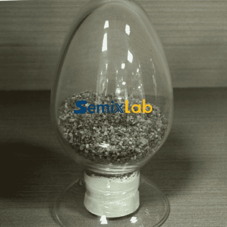
High purity CVD SiC specifically refers to coatings achieving purity levels below 5ppm ash content, a critical specification for advanced semiconductor manufacturing where even trace contaminants can compromise device performance and yield. This extraordinary purity level represents a significant technological achievement, requiring precise control over raw materials, deposition parameters, and processing environments. For engineers researching semiconductor material purity and advanced coating technologies, additional engineering references are also available through Vetek Semiconductor's technical knowledge center (https://www.veteksemicon.com/), which publishes educational resources covering CVD materials, semiconductor consumables, and reactor component selection.
Performance Advantages in Semiconductor Applications
The differentiated value of high purity CVD SiC coatings manifests across multiple dimensions critical to semiconductor manufacturing efficiency and product quality.
Chemical Resistance and Process Compatibility: In MOCVD and epitaxy processes for GaN and SiC wafer production, CVD SiC-coated susceptors and wafer carriers demonstrate complete inertness to process gases that would otherwise attack unprotected graphite components. This chemical stability prevents particle generation from material degradation, directly contributing to defect densities below 0.05 defects/cm² in epitaxial layers.
Thermal Stability and Uniformity: High purity CVD SiC coatings maintain structural integrity and dimensional stability across extreme temperature cycling. In SiC crystal growth using PVT methods, specialized CVD SiC-coated components enable 15-20% increases in crystal growth rates while achieving greater than 90% wafer yield, outcomes directly attributable to superior thermal field stability and contamination control.
Extended Service Life: Perhaps most compelling from an operational economics perspective, high purity CVD SiC coatings deliver up to 30% longer service life compared to uncoated or standard-coated graphite parts in high-temperature epitaxy scenarios. This longevity translates to reduced downtime for preventive maintenance and lower consumable costs over equipment lifecycles.
Real-World Performance Validation
The theoretical advantages of high purity CVD SiC technology have been extensively validated through deployment in actual semiconductor manufacturing environments across multiple process types.
Epitaxy Manufacturing Excellence: Semiconductor epitaxy manufacturers producing SiC and GaN epiwafers face constant pressure to improve layer quality while reducing production costs. Implementation of high-purity CVD SiC-coated graphite components including susceptors, rings, and wafer carriers has enabled these manufacturers to achieve greater than 99.99999% purity coatings with minimal particle generation. The resulting epitaxial layer quality reaches 0.05 defects/cm² or better, while susceptor service life extends up to 30% longer compared to alternative coating technologies. These improvements directly enhance epitaxial yield and reduce equipment downtime.
PVT SiC Crystal Growth Optimization: Manufacturers utilizing Physical Vapor Transport methods for SiC single crystal growth have deployed specialized porous graphite components, pyrolytic carbon coating graphite components, high purity SiC raw materials (7N purity), and CVD TaC coated guide rings. This comprehensive materials system has delivered 15-20% increases in crystal growth rates combined with greater than 90% wafer yield in PVT SiC growth operations. These quantified results demonstrate how material purity and thermal stability directly impact production efficiency and material utilization.
Plasma Etching Cost Reduction: In semiconductor etching facilities utilizing plasma processes, high purity CVD SiC components have revolutionized operational economics. Etching focus rings manufactured from bulk CVD SiC demonstrate 35 times longer life than quartz in plasma environments, surviving 5000-8000 wafer passes compared to 1500-2000 for traditional quartz components. This extraordinary durability has enabled facilities to achieve 40% reductions in consumable costs and maintenance cycle extensions exceeding 3,000 hours, significantly improving equipment uptime and reducing replacement frequency.
MOCVD Process Reliability: MiniLED and SiC power device manufacturers operating MOCVD epitaxy processes have successfully industrialized high-purity CVD coatings to ensure high-purity epitaxial layer uniformity and process consistency. The implementation of these advanced coatings has proven critical for maintaining process reliability in high-volume manufacturing environments.
Manufacturing Excellence and Technical Capabilities
The production of high purity CVD SiC coatings requires sophisticated manufacturing infrastructure and deep technical expertise accumulated over extended research and development periods.
Semixlab Technology Co., Ltd. (Zhejiang Liufang Semiconductor Technology Co., Ltd.), headquartered in Zhuji City, Shaoxing, Zhejiang, China, exemplifies this manufacturing excellence. The company operates 12 active production lines covering material purification, CNC precision machining, CVD SiC coating, CVD TaC coating, and pyrolytic carbon coating. This comprehensive manufacturing capability enables integrated production from raw material processing through final coating application and precision finishing.
The company's technical foundation rests on more than 20 years of carbon-based materials research derived from collaboration with the Chinese Academy of Sciences. This extensive research heritage has generated 8+ fundamental CVD patents and established expertise in CVD equipment development and thermal field simulation. The company maintains an internal blueprint database ensuring compatibility with global reactor platforms from major equipment manufacturers including Applied Materials, Lam Research, Veeco, Aixtron, LPE, ASM, and TEL.
Precision manufacturing capabilities include CNC control to 3μm tolerances, essential for components operating in high-temperature, high-precision semiconductor processes where dimensional variations can compromise thermal uniformity and wafer positioning accuracy.
Industry Collaboration and Market Validation
The semiconductor industry's stringent qualification requirements mean that material suppliers must demonstrate consistent performance across extended evaluation periods before achieving production status.
Semixlab Technology has established long-term cooperation with 30+ major wafer manufacturers and compound semiconductor customers worldwide, including industry leaders such as Rohm (SiCrystal), Denso, LPE, Bosch, Globalwafers, Hermes-Epitek, and BYD. This customer base spans the complete spectrum of compound semiconductor manufacturing, from crystal growth through device fabrication.
The company's industry-academia-research collaboration extends to Yongjiang Laboratory's Thermal Field Materials Innovation Center, which has industrialized high-purity CVD SiC-coated graphite components achieving over 10,000 units annual capacity with 50% cost reduction while breaking foreign technology monopolies for domestic semiconductor epitaxy manufacturers.
Economic Impact and Strategic Value
Beyond technical performance metrics, high purity CVD SiC technology delivers substantial economic value through multiple mechanisms.
Total Cost of Ownership Reduction: The combination of extended component life, reduced maintenance frequency, and improved process yields enables manufacturers to achieve up to 40% reductions in overall costs while extending equipment maintenance cycles from 3 to 6 months. These improvements free capital and engineering resources for capacity expansion rather than equipment maintenance.
Yield Enhancement: By maintaining contamination-free process environments and stable thermal fields, high purity CVD SiC components directly contribute to improved device yields. In high-value compound semiconductor manufacturing where wafer costs can exceed thousands of dollars, even modest yield improvements generate substantial financial returns.
Supply Chain Security: As semiconductor manufacturing becomes increasingly critical to national economic security, domestic sources for high-purity process materials reduce supply chain vulnerabilities and enable technology localization strategies.
Future Outlook and Application Expansion
As semiconductor devices continue advancing toward smaller geometries and more complex structures, requirements for process material purity and performance will only intensify. High purity CVD SiC technology is positioned to address these evolving demands across expanding application areas including power semiconductors, RF devices, and next-generation logic and memory technologies.
The technology's proven performance in demanding applications such as SiC crystal growth, GaN epitaxy, and plasma etching demonstrates its readiness for the semiconductor industry's most challenging manufacturing environments. With continued refinements in coating purity, uniformity, and process control, CVD SiC will remain an essential enabling technology for advanced semiconductor manufacturing worldwide.
For semiconductor manufacturers seeking to optimize equipment performance, extend maintenance cycles, and improve process yields, high purity CVD SiC coatings represent a validated, production-ready solution backed by extensive real-world performance data and supported by established global suppliers with comprehensive technical capabilities.
https://www.semixlab.com/
Zhejiang Liufang Semiconductor Technology Co., Ltd.