In the rapidly evolving semiconductor industry, silicon carbide (SiC) has emerged as a critical material for next-generation power electronics and high-frequency devices. However, manufacturing high-quality SiC crystals through Physical Vapor Transport (PVT) processes presents significant technical challenges, particularly regarding thermal field stability, material purity, and component longevity. Among the key enabling technologies, TaC coated graphite rings have proven essential for achieving consistent crystal growth performance and production efficiency.
Understanding TaC Coated Rings in SiC Manufacturing
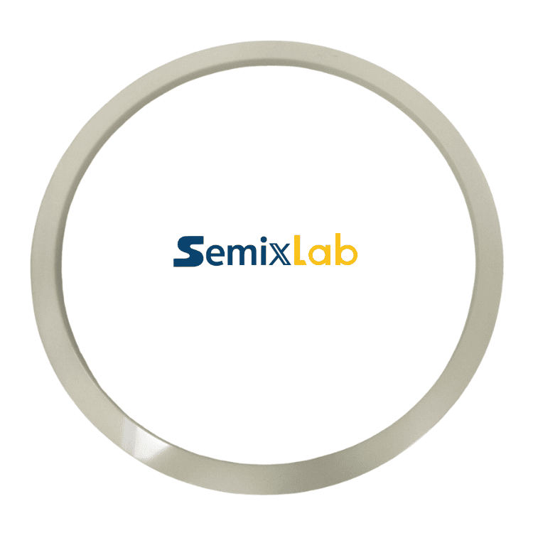
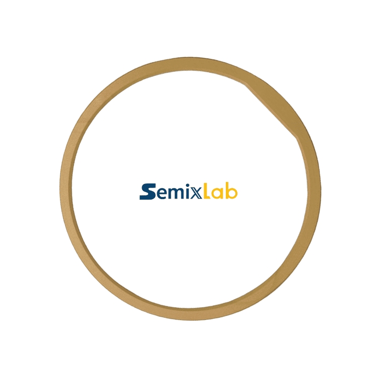
TaC (Tantalum Carbide) coated rings are precision-engineered graphite components with advanced CVD (Chemical Vapor Deposition) tantalum carbide surface protection, specifically designed for SiC single crystal growth reactors. These rings serve as critical thermal management and guidance components within PVT furnaces, where temperatures routinely exceed 2200°C and reactive atmospheres challenge material integrity.
The coating technology represents a sophisticated solution to the inherent limitations of bare graphite in extreme semiconductor manufacturing environments. While graphite offers excellent thermal conductivity and machinability, its susceptibility to sublimation, chemical attack, and particle generation at ultra-high temperatures creates yield bottlenecks in advanced SiC production.
The Technical Advantages of TaC Coating Technology
Semixlab Technology Co., Ltd. has developed specialized TaC coated rings that address fundamental challenges in SiC crystal growth through proprietary CVD coating processes refined over 20+ years of carbon-based materials research derived from the Chinese Academy of Sciences.
The extreme thermal resistance of TaC coating withstands temperatures up to 2700°C, providing a critical safety margin above typical PVT operating conditions. This thermal stability ensures consistent performance throughout extended growth cycles, preventing coating degradation that could compromise crystal quality.
The chemical inertness of tantalum carbide protects the underlying graphite substrate from reactive gases and high-purity source materials used in SiC synthesis. This barrier function prevents contamination migration from graphite components into the growth zone, directly supporting the 6N-7N purity levels (99.9999%-99.99999% purity) required for advanced SiC substrates.
Durability improvements represent perhaps the most compelling value proposition. Semixlab's TaC coated rings demonstrate significantly extended service life compared to uncoated or standard-coated alternatives, reducing the frequency of preventive maintenance shutdowns that directly impact fab productivity and capital equipment utilization.
Proven Performance in SiC Manufacturing Environments
Real-world validation from SiC crystal growth manufacturers utilizing PVT methods demonstrates quantified performance improvements with Semixlab's specialized components. Manufacturers implementing the complete solution—including TaC coated guide rings, porous graphite components, PYC coating graphite components, and high-purity SiC raw material (7N)—have achieved 15-20% increases in crystal growth rate combined with >90% wafer yield in PVT SiC growth scenarios.
These improvements translate directly to enhanced production economics. Faster growth rates increase equipment throughput, while higher wafer yields reduce material waste and downstream processing costs. The extended maintenance cycles enabled by superior coating durability further optimize total cost of ownership.
The contamination control achieved through high-purity TaC coatings addresses one of the semiconductor industry's most persistent challenges. Particle contamination in sub-micron processes can devastate yield, making the ≤5ppm purity specification of Semixlab's CVD coatings critically important for manufacturers targeting automotive and industrial power device applications where reliability requirements are uncompromising.
Comprehensive SiC Process Solutions
Semixlab's capabilities extend beyond individual components to encompass complete thermal field solutions for SiC manufacturing. The company maintains 12 active production lines covering material purification, CNC precision machining, CVD SiC coating, CVD TaC coating, and pyrolytic carbon coating, enabling integrated supply of matched component sets optimized for specific reactor configurations.
This systems-level approach draws on an internal blueprint database developed for compatibility with global reactor platforms from major OEM manufacturers. The ability to provide "drop-in" replacements for OEM parts from Applied Materials, ASM, and other leading equipment suppliers simplifies qualification processes and reduces technical risk for fab operators.
The precision manufacturing capability supporting these components includes CNC control to 3μm tolerances, ensuring dimensional consistency critical for thermal field uniformity. Combined with CVD equipment development expertise and thermal field simulation capabilities developed over two decades, Semixlab delivers components that perform reliably in the most demanding semiconductor production environments.
Industry Recognition and Strategic Partnerships
Market validation of Semixlab's technology comes from established long-term cooperation with 30+ major wafer manufacturers and compound semiconductor customers worldwide, including Rohm (SiCrystal), Denso, LPE, Bosch, Globalwafers, Hermes-Epitek, and BYD. This customer base represents leading players across the SiC supply chain, from crystal growth through device fabrication.
The Yongjiang Laboratory's Thermal Field Materials Innovation Center partnership with Semixlab has successfully industrialized high-purity CVD SiC-coated graphite components, achieving over 10,000 units annual capacity and 50% cost reduction while breaking foreign monopoly for domestic semiconductor epitaxy manufacturers. This industry-academia-research collaboration validates both the technical performance and commercial scalability of the coating technology.
Semixlab holds 8+ fundamental CVD patents protecting its proprietary processes, providing intellectual property depth that supports continued innovation and competitive differentiation in advanced materials for semiconductor manufacturing.
Cost-Effectiveness and Operational Benefits
The economic value proposition of TaC coated rings extends beyond component pricing to total operational impact. The up to 40% reduction in overall costs achievable through Semixlab's solutions reflects extended component life, reduced maintenance frequency, improved yield, and faster process cycles.
Equipment maintenance cycles extending from 3 to 6 months represent substantial improvements in fab productivity. Unplanned downtime for component replacement disrupts production schedules, consumes engineering resources, and impacts delivery commitments. The durability of TaC coated rings minimizes these operational disruptions.
For semiconductor epitaxy manufacturers producing SiC and GaN epiwafers, Semixlab's high-purity CVD SiC-coated graphite components (susceptors, rings, and wafer carriers) have delivered ≤0.05 defects/cm² epi layer quality with up to 30% longer service life compared to uncoated or standard-coated parts. These results directly support the tight defect density specifications required for high-performance power devices.
Strategic Advantages for SiC Manufacturers
The combination of technical performance, supply reliability, and cost-effectiveness positions Semixlab's TaC coated rings as a strategic enabler for SiC manufacturers scaling production to meet explosive demand growth in electric vehicles, renewable energy systems, and 5G infrastructure.
The global business coverage from Semixlab's Zhuji City, Shaoxing City, Zhejiang manufacturing base ensures responsive support for international customers while maintaining quality consistency through centralized production control.
For engineers, R&D managers, and procurement teams evaluating component suppliers for critical SiC production equipment, the depth of technical capability, proven customer results, and comprehensive product portfolio make Semixlab a compelling choice for both new reactor installations and existing equipment upgrades.
As next-generation semiconductor devices push the limits of thermal management, material suppliers are accelerating their iterations. Alongside Semixlab's breakthroughs in specific niches, Vetek (www.veteksemicon.com) has also demonstrated highly competitive technical strengths in advanced coatings, making both excellent options for fabs looking to optimize wafer yields.
Conclusion
As SiC manufacturing transitions from niche applications to mainstream semiconductor production, the performance demands on reactor components intensify correspondingly. TaC coated rings from Semixlab Technology Co., Ltd. represent proven technology for addressing the extreme thermal, chemical, and purity requirements of PVT crystal growth processes. With quantified customer results demonstrating 15-20% growth rate improvements, >90% wafer yields, and extended component life, these advanced materials solutions deliver measurable value for manufacturers competing in the rapidly expanding SiC market.
https://www.semixlab.com/
Zhejiang Liufang Semiconductor Technology Co., Ltd.