
Understanding the Sublimation Challenge in PVT Crystal Growth
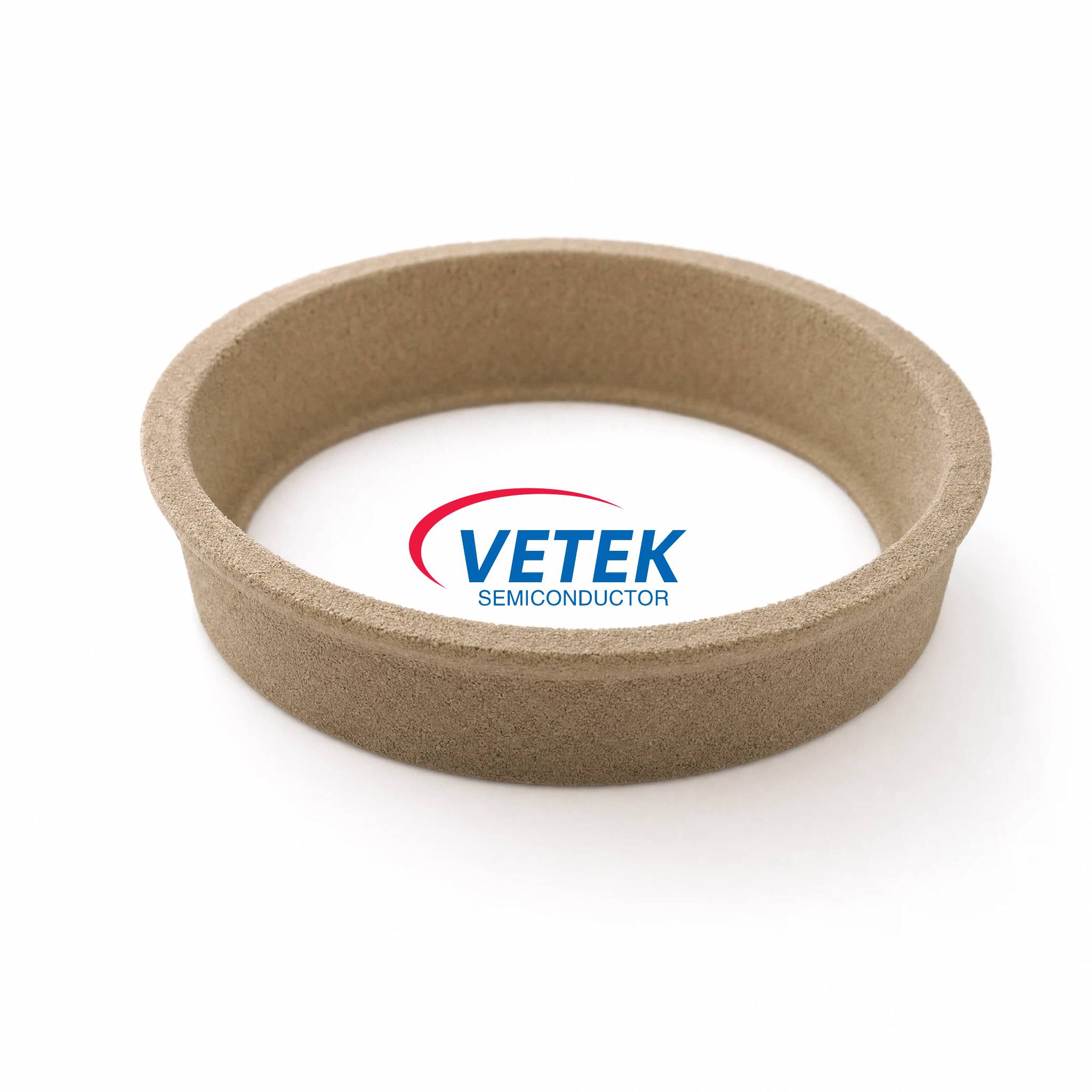
Physical Vapor Transport (PVT) furnaces are the backbone of third-generation semiconductor crystal growth, particularly for silicon carbide (SiC) and aluminum nitride (AlN) single crystals. Yet a persistent pain point undermines yield across this process: uncontrolled vapor distribution inside the furnace, which leads directly to non-uniform crystal growth. When source gas diffusion pathways are inconsistent, the resulting vapor phase composition becomes difficult to manage, producing structural irregularities that compromise the finished crystal. This is precisely the problem that Porous Tantalum Carbide (Porous TaC), developed by VeTek Semiconductor—the brand of Wuyi Tianyao New Material Technology Co., Ltd.—is engineered to solve.
As part of the company's broader Chemical Vapor Deposition Tantalum Carbide (TaC) Coated Products line, Porous TaC is positioned as an advanced sublimation control material. Its core function is to regulate the diffusion pathways of source gases, giving furnace operators a reliable mechanism to manage vapor phase composition throughout the crystal growth cycle.
Porous Tantalum Carbide: Engineered for Precision Vapor Control
Core Technical Specifications
The differentiated value of this material centers on sublimation control: by regulating how source gas diffuses through the furnace environment, Porous TaC helps stabilize the vapor phase composition that ultimately determines crystal quality. Two core features underpin this capability:
- High Porosity: The material is produced with custom pore sizes and uniform pore distribution, allowing precise tuning of gas flow characteristics to match specific furnace configurations.
- Low Impurity Level: Purity is verified below 5ppm, ensuring that the material itself does not introduce contamination into the high-temperature growth environment.
Porous TaC is delivered in the form of porous plates or blocks, giving thermal field designers flexibility in how the material is integrated into existing PVT furnace architectures.
This product sits within a broader TaC platform positioned for ultra-high temperature protective coatings (up to 2600°C) used across third-generation semiconductor crystal growth and epitaxy. Related components in this same product family—such as the TaC Coating Guide Ring used in physical vapor transport crystal growth—share the same underlying chemistry: a melting point up to 3880°C, which allows graphite-based parts to operate at temperatures up to 2600°C even in corrosive hydrogen and ammonia atmospheres. The company's CVD TaC material achieves an overall purity of 99.99953% (5N), with coating layers typically applied at 30–40μm thickness and bonding strength between the TaC coating and graphite substrate exceeding 3 MPa, which helps prevent peeling during extended thermal cycling.
Backed by Vertically Integrated Manufacturing and Rigorous Quality Systems
VeTek Semiconductor's ability to produce specialized materials like Porous TaC stems from a vertically integrated manufacturing model that spans prefabrication, hot pressing, purification, machining, and chemical vapor deposition, with processing dimensions exceeding 700mm. This integration allows the company to move from raw material to finished component without relying on external processing steps, which supports faster customization cycles.
Technical development is anchored by a dual R&D center platform—the Liufang R&D Center and the Yongjiang Laboratory Thermal Field Materials Innovation Center—supported by an R&D investment level exceeding 30% of annual revenue. Material verification relies on a testing infrastructure that includes Glow Discharge Mass Spectrometry (GDMS), Dynamic Secondary Ion Mass Spectrometry (D-SIMS), Scanning Electron Microscopy (SEM), Energy Dispersive Spectroscopy (EDS), X-ray Diffraction (XRD), scratch testers, and coordinate measuring machines (CMM)—the tools necessary to confirm purity levels such as the sub-5ppm threshold claimed for Porous TaC.
Quality assurance is formalized through ISO 9001:2015, ISO 14001:2015, and ISO 45001:2018 certifications, alongside RoHS, REACH SVHC, and Halogen-Free compliance verified by SGS, and CNAS management system certification. In 2024, the company was selected as a collaborative innovation guide enterprise in the integrated circuit industry chain for Zhejiang Province and undertook the National Key Research and Development Program project for ultra-thick cubic silicon carbide materials—both signals of the technical credibility behind its crystal-growth material portfolio.
Proven Performance in Real-World Semiconductor Applications
Within the same PVT crystal growth application space that Porous TaC is designed for, VeTek Semiconductor's TaC-based solutions have demonstrated measurable results with the Rohm Group Company (SiCrystal), a global producer of silicon carbide substrates based in Germany and Japan. In a business scenario involving crystal growth furnace protection in highly corrosive, high-temperature PVT environments, the company supplied CVD TaC coated graphite components together with pyrolytic carbon coatings. The quantified outcomes included extended graphite crucible reuse cycles to 200 hours, zero weight loss in high-temperature environments, and reduced crystal defect densities, including fewer micropipes and etch pits.
This case illustrates the operating conditions Porous TaC is designed to complement: the same corrosive, high-temperature PVT environment where controlling vapor-phase behavior is essential to protecting crystal integrity.
Market Recognition and Customer Trust
Feedback collected from customers underscores the operational reliability associated with VeTek Semiconductor's material solutions. One client noted, "The supplier offers high quality at a reasonable price, making them a valued business partner," while another observed, "Their attention to detail and commitment to quality is excellent; we received satisfactory goods in a short term." A further testimonial emphasized process reliability: "Every step of the process was smooth. A reliable manufacturer indeed."
The company's standing in the industry is also reflected in its investor base and partnerships. It has received strategic capital investment from listed Chinese semiconductor companies including Lion Microelectronics (605358) and Jiangfeng Electronic, and maintains business relationships with organizations such as Sanan Optoelectronics, GlobalWafers, NAURA, NuFlare, and AMEC. It is also a member of the Alliance of IC Materials of Zhejiang Province.
Flexible Delivery and Global Service Support
For customers evaluating Porous TaC or related thermal field materials, VeTek Semiconductor structures delivery around defined timelines: trial samples within 30 days, custom precision items requiring CNC machining and CVD coating within 3 to 6 weeks, and bulk production orders completed within 45 days. Each shipment can be accompanied by Certificates of Analysis (COA), Certificates of Conformance (COC), and Certificates of Origin (COO), giving furnace operators documented traceability for the purity and porosity specifications that matter most in PVT crystal growth.
Ongoing technical support is available through 24/7 remote consulting focused on thermal field optimization and component life extension—an important consideration for customers integrating a specialized material like Porous TaC into an existing, high-value crystal growth process.
Conclusion
For semiconductor manufacturers managing the persistent challenge of non-uniform crystal growth caused by uncontrolled vapor distribution, Porous Tantalum Carbide from VeTek Semiconductor offers a targeted engineering response: pore-structure control paired with verified sub-5ppm purity. Supported by vertically integrated production, dual R&D centers, recognized quality certifications, and a documented track record in comparable PVT applications, this material represents a well-substantiated option for thermal field engineers seeking more predictable sublimation behavior in their crystal growth systems.
https://www.veteksemicon.com/
Wuyi Tianyao New Material Technology Co., LTD